Scientific Research · Memristors

Hybrid Memristors
Bismuth Perovskites & Emerging Materials

Comprehensive reference on resistive switching devices integrating lead-free bismuth-based perovskites, chalcogenides, and metal-oxide materials. From theoretical foundations to neuromorphic computing applications and market analysis.

13
Bismuth Compounds
10⁶
Max ON/OFF Ratio
$4.8B
Market by 2030
1971
Theoretical Prediction
30
Scientific References
Introduction

The Fourth Fundamental Circuit Element

A memristor (memory + resistor) is a two-terminal passive element whose resistance depends on the history of current or voltage applied. Predicted by Leon Chua in 1971 and physically demonstrated by HP Labs in 2008, memristors are now at the forefront of non-volatile memory and neuromorphic computing research.

Non-Volatility

Resistance state persists without power supply — from 10³ s (perovskites) to over 10 years (mature oxides).

Synaptic Plasticity

Analog conductance modulation mimics biological synapses — LTP/LTD over 100+ discrete levels for neuromorphic learning.

Ultra-Low Energy

Sub-volt operation (0.2–1.5 V), nanoampere read currents. Energy per operation below 1 fJ — orders of magnitude below CMOS.

Nanoscale Density

Filamentary switching at <10 nm confirmed. Integration density exceeds 10¹² bits/cm² in 3D crossbar architectures.

History

Timeline of Memristors (1971–2025)

From Chua's theoretical prediction to industrial joint ventures — 54 years of memristor science.

● Theory ● Breakthrough ● Fabrication ● Publication ● Industry
1971Theoretical PredictionTheory
Leon Chua (UC Berkeley) postulates the memristor as the 4th fundamental passive element, completing R, C, and L. [24]
1976Generalization to Memristive SystemsTheory
Chua and Kang extend the concept to higher-order memristive systems, opening the path to neural network applications. [24]
2008First Physical Memristor (HP Labs)Breakthrough
Strukov, Snider, Stewart, and Williams demonstrate a TiO₂ thin-film memristor, confirming Chua's theory after 37 years. [25]
2010First Crossbar ArraysFabrication
HP Labs and HRL Laboratories fabricate 64-bit TiO₂ crossbar matrices for logic computation. [14]
2012HfO₂ RRAM Reference PaperPublication
Wong et al. publish the landmark review on metal-oxide RRAM, establishing HfO₂ as the industrial standard. [22]
2013First Commercial ReRAM MCUIndustry
Panasonic launches the MN101L, the first mass-production microcontroller with embedded TaO₄ ReRAM (180 nm). [30]
2015Integrated Neuromorphic NetworkBreakthrough
Prezioso et al. demonstrate a trained and operational neural network on a memristor array, proven on image classification. [27]
2017Intel LoihiIndustry
Intel presents Loihi, a 128-core neuromorphic chip with on-chip learning, inspired by memristor research. [15]
20196 nm Crossbar ArrayBreakthrough
Pi et al. fabricate memristive crossbar arrays with 6 nm half-pitch and 2 nm critical dimension — a world record. [26]
2020Full CNN on MemristorsBreakthrough
Yao et al. (Tsinghua) implement a complete convolutional neural network entirely on memristors, validating compute-in-memory. [28]
2023Bi Perovskite MemristorsBreakthrough
Zhang et al. demonstrate lead-free Cs₃Bi₂I₉ memristors for neuromorphic computing with ON/OFF ratio >10⁵. [1]
2024Flexible Bismuth Perovskite MemristorsFabrication
Yoo et al. fabricate flexible bismuth memristors with improved endurance on PEN substrate, enabling soft IoT. [5]
2025SAIMEMORY — Intel/SoftBank Joint VentureIndustry
SAIMEMORY founded (SoftBank + Intel + University of Tokyo) for memristive AI accelerators, ~$20M capital. [19]
Physics

I–V Characteristics & Hysteresis

The memristor's signature is a pinched hysteresis loop in the I-V plane — resistance depends on the history of applied current or voltage.

V I V_SET V_RESET LRS (R_ON) HRS (R_OFF) SET RESET 0

Fig. 1 — Pinched hysteresis loop: LRS (RON) in violet, HRS (ROFF) in blue. The loop always passes through the origin.

SET Transition

When voltage exceeds VSET, conductive filament forms (metal cations or oxygen vacancies migrate) — device switches from HRS to LRS. Compliance current Icc limits filament diameter.

RESET Transition

Applying opposite bias (or exceeding VRESET) dissolves the filament — device returns to HRS. RESET is typically a gradual analog process, while SET is more abrupt.

Switching Mechanisms

  • VCM (Valence Change): O²⁻ vacancy migration — HfO₂, TiO₂, Ta₂O₅
  • ECM/CBRAM: Electrochemical metal (Ag/Cu) filament — Cu/Al₂O₃, Ag/MoS₂
  • Halide migration: I⁻, Br⁻, Cl⁻ — Cs₃Bi₂I₉, Cs₃Bi₂Br₉
  • PCM: Amorphous/crystalline phase — GeSe, GST
  • Ferroelectric: Polarization reversal — BaTiO₃
10²–10⁶
ON/OFF ratio
<1 ns
Switch speed
<1 fJ
Energy/op.
Classification

Memristor Types — 12 Materials

Comparative table of key memristor classes from mature metal oxides to emerging bismuth perovskites and chalcogenides.

Category Compound Structure Mechanism ON/OFF VSET (V) Endurance Retention Maturity
Metal OxideHfO₂Au/HfO₂/TiNO²⁻ vacancy migration10⁶0.710¹²10 yrsIndustrial
Metal OxideTiO₂Pt/TiO₂/PtO²⁻ ionic drift10³1.010⁹10 yrsIndustrial
Metal OxideTa₂O₅Pt/Ta₂O₅/TaOₓ/PtOxygen vacancies10⁴1.210¹²10 yrsAdvanced
Metal OxideAl₂O₃Cu/Al₂O₃/PtCu electrochemistry10⁶0.810⁶10⁵ sResearch
Bi PerovskiteCs₃Bi₂I₉Au/Cs₃Bi₂I₉/ITOI⁻ halide migration10⁵0.610⁴10⁴ sResearch
Bi PerovskiteCs₃Bi₂Br₉Au/Cs₃Bi₂Br₉/ITOBr⁻ halide migration10³0.810⁴10⁴ sResearch
Bi PerovskiteCs₃Bi₂Cl₉Au/Cs₃Bi₂Cl₉/ITOCl⁻ halide migration10⁴1.510³10³ sEmerging
Pb PerovskiteMAPbI₃Au/MAPbI₃/ITOI⁻ + Pb²⁺ migration10⁶0.310³10³ sResearch
ChalcogenideMoS₂Ag/MoS₂/AuS vacancies + Ag filaments10⁶0.210⁵10⁴ sResearch
ChalcogenideGeSeCu/GeSe/PtAmorphous/crystalline10⁴0.310⁸10 yrsAdvanced
OrganicPEDOT:PSSAu/PEDOT/ITOIonic doping10²0.510⁶10⁴ sResearch
FerroelectricBaTiO₃Pt/BaTiO₃/SrRuO₃Ferroelectric polarization10⁴1.510⁹10 yrsAdvanced
Properties

8 Key Properties of Bismuth-Based Memristors

Non-Volatility

Resistance state is retained without power. Retention ranges from 10³ s (perovskites) to over 10 years (mature oxides), enabling persistent memory with near-zero standby power consumption.

Retention >10⁴ s

Synaptic Plasticity

Analog conductance modulation mimics biological synapses. Bismuth memristors excel at LTP (Long-Term Potentiation) and LTD (Long-Term Depression) over 100+ distinct levels — essential for neuromorphic learning.

>100 analog levels

Ultra-Fast Switching

Transition time between resistive states is in the nanosecond range. Metal oxides achieve <1 ns; bismuth perovskites ~50 ns. Fast switching is essential for high-frequency neuromorphic applications.

<100 ns typical

Ultra-Low Power

Sub-volt operation (0.2–1.5 V) with nanoampere read currents. Energy × time per operation falls below 1 fJ — several orders of magnitude below CMOS transistors.

<1 fJ per operation

Nanometric Scalability

Operation validated down to <10 nm dimensions thanks to filamentary switching. Scalability exceeds CMOS limits and enables integration densities exceeding 10¹² bits/cm² in 3D crossbar architectures.

Nodes <10 nm

Eco-Compatibility

Bismuth-based materials are abundant, non-toxic, and recyclable. Unlike lead perovskites, they present no environmental hazard and comply with RoHS standards and green manufacturing processes.

Lead-free, no rare earths

Thermal Stability

Reliable operation over wide temperature ranges. Bismuth perovskites remain stable up to 250°C (<5% degradation over 1000h at 85°C), ensuring reliability in harsh environments and embedded applications.

Stable up to 250°C

High Endurance

Capacity to sustain millions of SET/RESET cycles without significant degradation. Mature oxides exceed 10¹² cycles; bismuth perovskites reach 10⁴ cycles with continuously improving cycle-to-cycle variability.

10⁴–10¹² cycles
Materials

Bismuth-Based Memristors — 13 Compounds

Lead-free bismuth compounds span three structural families, offering a bandgap range of 0.3–3.0 eV and diverse switching mechanisms.

13 compounds
·
3 structural families
·
Bandgap: 0.3–3.0 eV
·
Lead-free · RoHS compliant
Ternary Perovskites A₃Bi₂X₉ 5 compounds
CompoundBandgap (eV)Structure/TypeON/OFFKey Properties
Cs₃Bi₂I₉2.050D dimer clusters10⁵Best ON/OFF ratio; excellent neuromorphic behavior; LTP/LTD over 100 levels [1,3]
Cs₃Bi₂Br₉2.620D dimer clusters10³Stable LTP/LTD synaptic emulation; artificial synapse with >50 states [2,8]
Cs₃Bi₂Cl₉3.020D dimer clusters10⁴Widest bandgap; higher V_SET; good for UV-active devices [2]
MA₃Bi₂I₉2.100D / layered10³Methylammonium-based; stable at room temperature; flexible substrate compatible [1]
(NH₄)₃Bi₂I₉2.080D dimer10³Inorganic-organic hybrid; low-temperature processing; printable [2]
Double Perovskites A₂M'BiX₆ 3 compounds
CompoundBandgap (eV)Structure/TypeON/OFFKey Properties
Cs₂AgBiBr₆1.953D double perovskite10⁴Best thermal stability among Bi perovskites; long-term retention >10⁵ s [2,6]
Cs₂AgBiCl₆2.773D double perovskite10³Wide bandgap; high transparency; suitable for transparent memristors [2]
Ag₃BiI₆1.852D layered10⁴Narrow bandgap; moisture-stable 2D structure; solution-processable [6]
Oxides, Chalcogenides & Binary Compounds 5 compounds
CompoundBandgap (eV)Structure/TypeON/OFFKey Properties
Bi₂O₃2.85Monoclinic oxide10⁴Mature material; CMOS-compatible sputtering; stable under ambient [9]
BiFeO₃2.67Rhombohedral perovskite10⁵Ferroelectric + memristive; multiferroic; domain wall switching [3]
Bi₂S₃1.30Orthorhombic10³Narrow bandgap chalcogenide; photoresponsive; flexible [4]
Bi₂Se₃0.30Topological insulator10²Topological surface states; low V_SET; ultra-thin film compatible [4]
BiOI1.77Tetragonal10³Unique oxysulfide; visible-light absorption; humidity sensor integration [3]
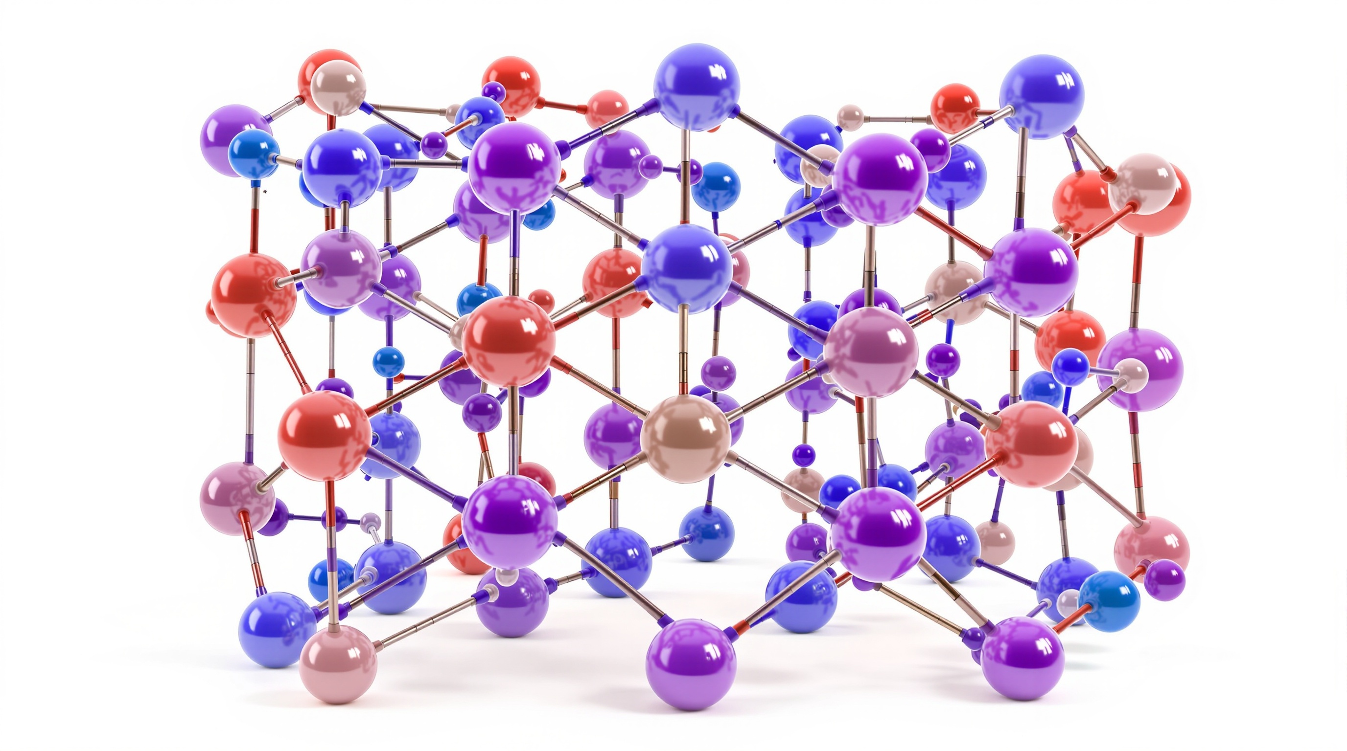
Bismuth perovskite crystal structure — Cs₃Bi₂I₉ halide perovskite

Cs₃Bi₂I₉ perovskite crystal

Methods

Fabrication Methods — 6 Techniques

From laboratory spin-coating to industrial-scale atomic layer deposition and inkjet printing — each method has its niche.

Spin Coating

Centrifugal deposition of precursor solution onto substrate. Simple, fast, and inexpensive — ideal for bismuth perovskites. Controllable thickness from 20 to 500 nm.

Temperature
<150°C
Thickness
20–500 nm
Materials
Cs₃Bi₂I₉, Cs₃Bi₂Br₉, PEDOT:PSS, MAPbI₃
Low costSimple<1 min depositR&D ideal Limited uniformityNot scalable >6">90% material loss

Sputtering (DC/RF)

Argon ion bombardment of a target in plasma ejects atoms that deposit on the substrate. Mature technique for metal oxides.

Temperature
25–400°C
Thickness
5–200 nm
Materials
HfO₂, TiO₂, Ta₂O₅, Al₂O₃, ITO
Excellent uniformityReproducibleIndustrial High costMulti-component complex

ALD (Atomic Layer Deposition)

Layer-by-layer atomic deposition via sequential gaseous precursor cycles. Unmatched sub-nanometer precision for ultra-thin layers.

Temperature
100–350°C
Thickness
1–50 nm
Materials
HfO₂, TiO₂, Al₂O₃, ZnO
Atomic controlPerfect 3D conformalityReproducible Very slow (~1 Å/cycle)Expensive

CVD (Chemical Vapor Deposition)

Chemical reaction of gaseous precursors at the heated substrate surface. Widely used for 2D materials and chalcogenides.

Temperature
200–900°C
Thickness
1–100 nm
Materials
MoS₂, GeSe, Bi₂S₃, graphene
High crystalline qualityScalableUniform films High temperatureToxic byproducts

Thermal Evaporation

Heating source material under high vacuum until evaporation, then condensation on the substrate. Classical method for metal electrodes.

Temperature
Substrate <100°C
Thickness
10–200 nm
Materials
Au, Ag, Al, Cu (electrodes)
SimpleHigh purityBest for metals Poor step coverageAlloys difficult

Inkjet Printing

Additive deposition of nanometric droplets of functional ink on the substrate. Emerging technique for flexible electronics and memristive circuits on paper.

Temperature
<200°C
Thickness
50–500 nm
Materials
Bi perovskites, TiO₂ nanoparticles, chalcogenides
MasklessFlexible substratesUltra-low cost ~20 µm resolutionAnnealing required
Analysis

Performance Comparison

Quantitative comparison of memristor materials across ON/OFF ratio, endurance, and VSET.

ON/OFF Ratio (log₁₀ scale) by material

HfO₂
10⁶
Al₂O₃
10⁶
MoS₂
10⁶
MAPbI₃
10⁶
Cs₃Bi₂I₉
10⁵
Ta₂O₅
10⁴
Cs₃Bi₂Cl₉
10⁴
GeSe
10⁴
TiO₂
10³
Cs₃Bi₂Br₉
10³
PEDOT:PSS
10²
■ Metal Oxide ■ Bi Perovskite ■ Chalcogenide ■ Organic

Endurance (log₁₀ cycles)

HfO₂
10¹²
Ta₂O₅
10¹²
BaTiO₃
10⁹
TiO₂
10⁹
GeSe
10⁸
PEDOT:PSS
10⁶
Al₂O₃
10⁶
MoS₂
10⁵
Cs₃Bi₂I₉
10⁴
Cs₃Bi₂Br₉
10⁴
MAPbI₃
10³

⚠ Bismuth perovskites (10⁴) remain below industrial targets — active area of improvement in 2024–2025 research.

VSET (Volts) — Lower is better

MoS₂
0.2 V
MAPbI₃
0.3 V
GeSe
0.3 V
Cs₃Bi₂I₉
0.6 V
HfO₂
0.7 V
Al₂O₃
0.8 V
Cs₃Bi₂Br₉
0.8 V
PEDOT:PSS
0.5 V
TiO₂
1.0 V
Ta₂O₅
1.2 V
BaTiO₃
1.5 V

Research Publications by Material Class (2008–2024)

Year Oxides Perovskites Chalcogenides Hybrids
20083
201282
20161134
202012762
202412986

Relative publication count (normalized). Oxides plateau at maturity while perovskites and hybrids show the strongest growth (2022–2024).

Architecture

Crossbar Architectures

Crossbar arrays place memristors at each intersection of orthogonal word-line and bit-line grids — enabling extreme integration density and in-memory computation.

Crossbar array memristor chip — scanning electron microscope image
Memristor crossbar architecture diagram

Passive Crossbar (0T1R)

Direct wire intersection with one memristor. Maximum density but vulnerable to sneak-path currents that corrupt read operations in large arrays.

Highest density — 4F²/cell Sneak-path currents; limited array size

1T1R (Transistor + Memristor)

Each memristor paired with an access transistor that provides electrical isolation. Eliminates sneak paths; industrial standard for dense arrays.

High precision; large array size 2× footprint vs 0T1R; CMOS complexity

1S1R (Selector + Memristor)

Two-terminal nonlinear selector element in series with the memristor. Suppresses parasitic currents without a full transistor; compatible with 3D stacking.

Denser than 1T1R; 3D compatible Selector window limited; still developing

3D Stacked Crossbar

Multiple crossbar layers stacked vertically (BEOL integration). Multiplication of density per footprint area — Samsung V-NAND approach applied to RRAM.

Highest volumetric density; proven concept Thermal budget constraints; complex process

Hybrid Architectures — Perovskite + Chalcogenide Heterostructures

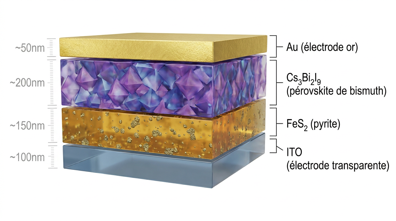
Multilayer memristive architectures combine bismuth perovskites (excellent neuromorphic analog behavior, low VSET) with chalcogenide layers (superior endurance, multi-level capability). The interfacial coupling between the two layers creates novel switching dynamics not available in either material alone. Fabricated by sequential spin-coating (Bi perovskite) + sputtering (chalcogenide), these heterostructures achieve 4–8 stable resistance levels per device for multi-bit storage. [6, 7]

4–8
Resistance levels/device
10⁵
Improved endurance
<150°C
Process temperature
2-bit
MLC storage / cell
Challenges

6 Key Technical Challenges

Remaining obstacles on the path from research prototype to commercial memristive technology.

Device-to-Device Variability

● Critical

The stochastic nature of conductive filament formation causes significant parameter variations (VSET, RON, ROFF) between identical devices on the same wafer — typically 10–30% for oxides and 15–40% for perovskites.

Mitigation: Controlled forming techniques, feedback circuits, periodic recalibration, fault-tolerant designs. [11, 13]

Sneak-Path Currents

● High

In passive crossbar arrays, parasitic currents through unselected memristors corrupt read operations and increase power consumption. This problem worsens exponentially with array size.

Mitigation: 1T1R or 1S1R cell architectures, nonlinear threshold cells, differential sensing schemes. [12, 14]

Endurance Degradation

● Moderate

Repeated SET/RESET cycles cause defect accumulation and gradual resistance drift. HfO₂ oxides reach 10¹² cycles but bismuth perovskites plateau at 10⁴ and chalcogenides at 10⁵ — insufficient for some high-frequency neuromorphic applications.

Mitigation: Interface engineering, encapsulation, optimized programming voltages, periodic refresh. [4, 5, 13]

Nonlinearity & Asymmetry

● Moderate

Synaptic weight updates (potentiation/depression) show nonlinearity and asymmetry that degrade neural network learning accuracy. The nonlinearity ratio can reach 3–5 for bismuth perovskites.

Mitigation: Optimized pulse schemes, variability-aware training algorithms, differential architectures (2 memristors per synapse). [8, 14]

CMOS Compatibility & Scalability

● High

BEOL integration imposes strict thermal constraints (<400°C). Bismuth perovskites are compatible (<200°C), but some CVD chalcogenides require >400°C. Scalability beyond the 10 nm node remains to be demonstrated for emerging materials.

Mitigation: Low-temperature sputtering, plasma-assisted ALD, layer transfer, direct printing. [6, 7, 13]

Long-Term Retention

● Moderate

Thermal relaxation of conductive filaments and ionic diffusion can degrade stored states. Perovskites suffer from spontaneous halide migration at room temperature, limiting retention to ~10⁴ s without optimization.

Mitigation: Diffusion barrier layers, engineered interfaces, hermetic encapsulation, periodic refresh for critical applications. [1, 3, 5]
Market

Memristor Market & Segments

Global memristor market projected to grow from $436M (2024) to $4.8B (2030) at 30–40% CAGR, driven by neuromorphic computing and RRAM adoption. [17, 18]

Market Growth ($M) — 2022–2030

2022
$220M
2024
$436M
2025
$620M
2026
$950M
2027
$1.45B
2028
$2.20B
2029
$3.30B
2030
$4.80B

CAGR ~30–40% (2024–2032). Sources: Grand View Research, Mordor Intelligence [17, 18]

Market Segments 2024

RRAM Memory
35%
Neuromorphic Computing
30%
Sensors & IoT
15%
Consumer Electronics
12%
Aerospace & Defense
8%

Key Market Milestones

2008HP Labs demonstrates first TiO₂ memristor
2013Panasonic launches first commercial ReRAM MCU
2025SAIMEMORY JV Intel/SoftBank for AI memristors (~$20M)
Products

Commercial Products & Advanced Prototypes

From Panasonic's first production MCU (2013) to Intel/SoftBank AI accelerators (2025) — the memristor industry is emerging.

Company Product Technology Node Year Status Application
PanasonicMN101L ReRAM MCUTaO₄ RRAM180 nm2013Mass ProductionIoT, wearables
FujitsuMB85AS12MTCBRAM (Cu/Al₂O₃)130 nm2019ProductionSmart meters, industry
SamsungEmbedded ReRAMHfO₂ OxRAM28 nm2022QualificationMCU, advanced IoT
Weebit NanoReRAM IPSiO₄ RRAM22 nm FDSOI2024IP LicenseEmbedded NVM
Crossbar Inc.CBRAM 40 nmCBRAM (Ag/a-Si)40 nm2023SamplesSecurity, Edge AI
4DS MemoryInterface Switching ReRAMPrCaMnO₄40 nm2024DevelopmentSCM, storage
Intel/SAIMEMORYMemristor AI AcceleratorRRAM CIM2025Joint VentureAI, compute-in-memory
BrainChipAkida•Neuromorphic + ReRAM22 nm2023ProductionEdge AI neuromorphic
Memory Technologies

Memory Technology Comparison

Where do RRAM/memristors fit in the memory landscape? Head-to-head comparison across all major technologies.

Property SRAM DRAM NAND Flash RRAM/Memristor PCM MRAM
Non-Volatile
Read Speed~1 ns~10 ns~50 µs~10 ns~50 ns~10 ns
Write Speed~1 ns~10 ns~1 ms<10 ns~50 ns~10 ns
Cell Size6F²6F²4F²/level4F²4F²6–20F²
Endurance10³–10⁵10⁴–10¹²10⁸>10¹⁵
Energy/op.~1 fJ~10 fJ~100 pJ<1 fJ~1 pJ~1 pJ
Multi-LevelMLC/TLC/QLC2–4 bit/cellPCM-MLC
3D StackableV-NAND 200+YesDevelopingLimited
CIM CapableLimitedLimitedExcellentModerateModerate
CMOS Compat.✓ FEOL✓ FEOL✓ FEOL✓ BEOL✓ BEOL✓ BEOL
MaturityMatureMatureMatureEmergingEmergingGrowing
RRAM's Key Advantage

Unique combination of BEOL integration + non-volatility + sub-10 ns speed + analog multi-level + compute-in-memory capability. No other technology matches all five simultaneously.

Global Semiconductor Memory

DRAM + NAND market: ~$207B (2026), growing to ~$430B by 2035. Samsung, SK Hynix, Micron control >90% of shares. Emerging technologies (RRAM, PCM, MRAM) represent ~1% but growing rapidly. [20]

HBM for AI

HBM (High Bandwidth Memory) grew +300% in 2024 driven by AI GPUs. SK Hynix holds >50% of the HBM3E market. Next generation: memristive in-memory computing may displace HBM for edge AI inference. [20]

Engineering

Device Engineering & Design

MIM (Metal–Insulator–Metal) stack design, process flow, and key design parameters for memristive devices.

MIM Stack Layers

Top Electrode (TE)
Au, Ag, TiN, Pt · 50–200 nm
Electrical contact; ionic reservoir (CBRAM). Au = inert (VCM); Ag/Cu = active (ECM). TiN = CMOS standard.
Switching Layer
HfO₂, TaOₓ, Cs₃Bi₂I₉, MoS₂ · 5–50 nm
Site of conductive filament formation/dissolution. Uniformity and thickness critically control performance. Optimal: 8–15 nm.
Interface Layer (optional)
Al₂O₃, TiOₓ sub-stoich. · 1–5 nm
Oxygen vacancy reservoir; reduces device-to-device variability by 30–50% in HfO₂/Al₂O₃ stacks.
Bottom Electrode (BE)
Pt, TiN, ITO, W · 50–200 nm
Electrical contact; diffusion barrier. ITO for transparent/flexible; Pt for lab reference; TiN = CMOS standard.
Substrate
Si/SiO₂, glass, PEN/PET (flexible)
Mechanical support and electrical isolation. Flexible substrates (PEN, PET) enable <150°C bismuth perovskite processing for soft electronics.
3D cross-section of an RRAM cell showing TE/switching layer/BE MIM stack

RRAM MIM cell — TE / switching layer / BE

8-Step Fabrication Process

1

Substrate Preparation

RCA clean (Si) or O₂ plasma (flexible). Thermal oxidation of 100 nm SiO₂ for insulation.

~30 min
2

Bottom Electrode Deposition

DC sputtering of TiN (20 nm adhesion) + Pt (100 nm) at 3 mTorr. Or ITO by RF sputtering for transparent devices.

~45 min
3

BE Lithography

E-beam litho (sub-100 nm) or UV photolitho (>µm). Defines parallel lines (bottom word lines).

~2 h
4

Switching Layer Deposition

ALD HfO₂ (10 nm, 200 cycles, 250°C) or spin-coating Cs₃Bi₂I₉ (2000 rpm, 30 s, 100°C anneal).

~1–4 h
5

Top Electrode Deposition

Thermal evaporation of Au (50 nm) or TiN sputtering (100 nm) through shadow mask or after litho.

~30 min
6

TE Lithography

Defines bit lines perpendicular to word lines. Lift-off or IBE/RIE etching.

~2 h
7

Passivation & Contacts

SiNₓ or Al₂O₃ encapsulation (PECVD/ALD). Contact pad opening by RIE etching.

~1 h
8

Forming & Characterization

Electroforming by voltage sweep. I-V, endurance, retention, and statistical variability characterization.

~2–8 h
V_SET optimal
≤1 V
sub-volt CMOS logic compatible
Compliance I_cc
10–100 µA
stability/energy tradeoff
Active area
50×50 nm²
to 10×10 µm²
Crossbar pitch
≤50 nm
>10¹¹ bits/cm²
Deposition T°
<350°C
BEOL compatible
Applications

Application Domains

Four major domains where memristive technology provides transformational advantages over conventional electronics.

Neuromorphic brain-chip with memristor synaptic array for artificial neural network computing

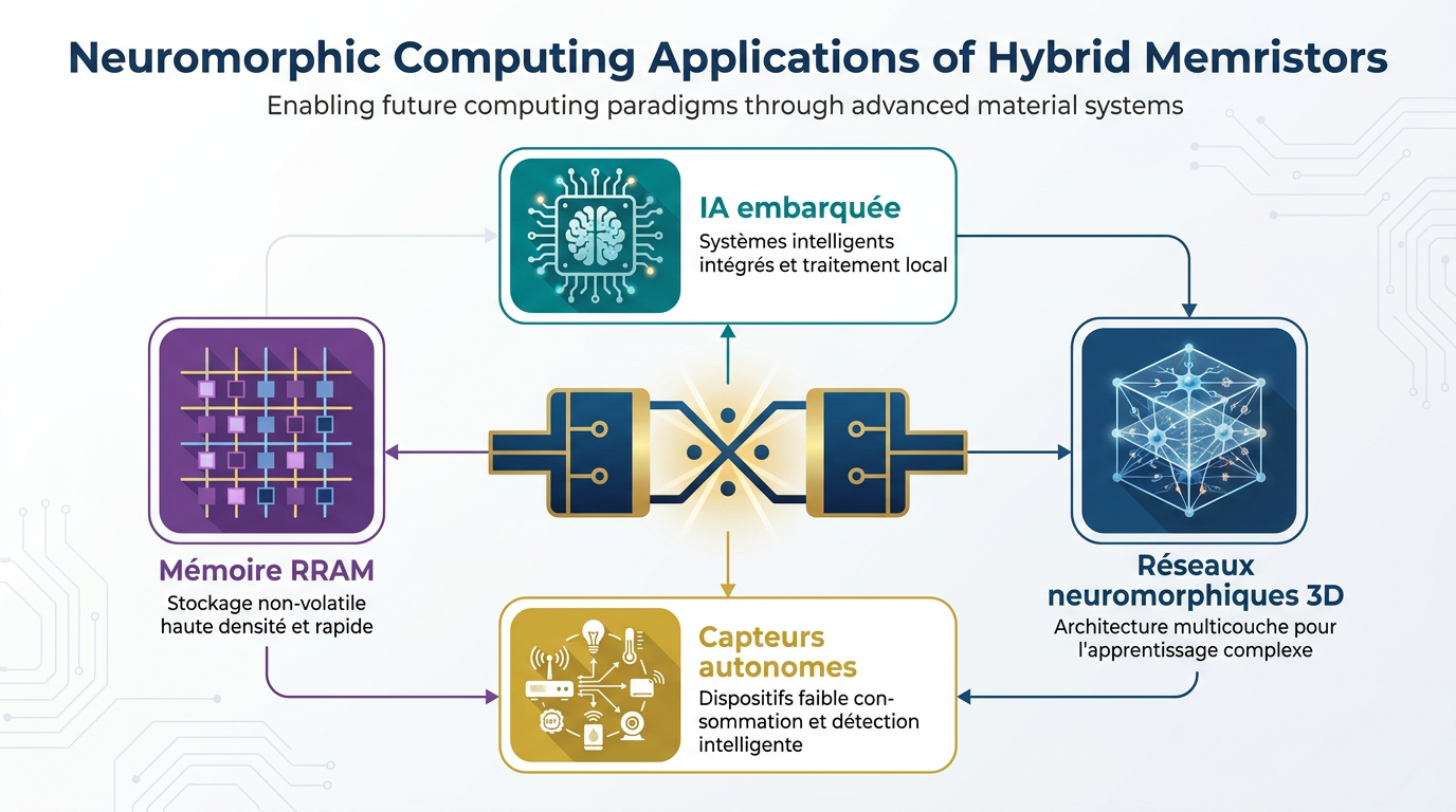
Neuromorphic Computing

Memristors act as artificial synapses in spiking neural networks. Bismuth perovskite devices demonstrate 100+ conductance levels, LTP/LTD synaptic plasticity, and STDP (Spike-Timing-Dependent Plasticity) — enabling on-chip learning that mirrors biological neurons. Energy consumption: <1 pJ per synaptic event. [15, 27, 28]

Compute-in-Memory (CIM)

Matrix-vector multiplications performed directly in the memristor crossbar array without data movement — eliminating the von Neumann bottleneck. Demonstrated: full CNN inference on memristor arrays with 100× lower energy than GPU [28, 29]. Key for edge AI acceleration.

Hardware Security (PUF/RNG)

The stochastic nature of filament formation creates unique, unclonable physical fingerprints (PUF — Physical Unclonable Functions). Each device's "fingerprint" is generated by quantum-level randomness, providing cryptographic keys that cannot be reverse-engineered. Also used for true random number generation (TRNG). [13]

Flexible & Wearable Electronics

Bismuth perovskite memristors fabricated by spin-coating at <150°C are fully compatible with flexible polymer substrates (PEN, PET, Kapton). Applications: wearable biosensors with embedded analog memory, e-skin neuromorphic patches, disposable smart labels with write-once memory. [5, 16]

Memristor applications infographic — neuromorphic, CIM, security, IoT
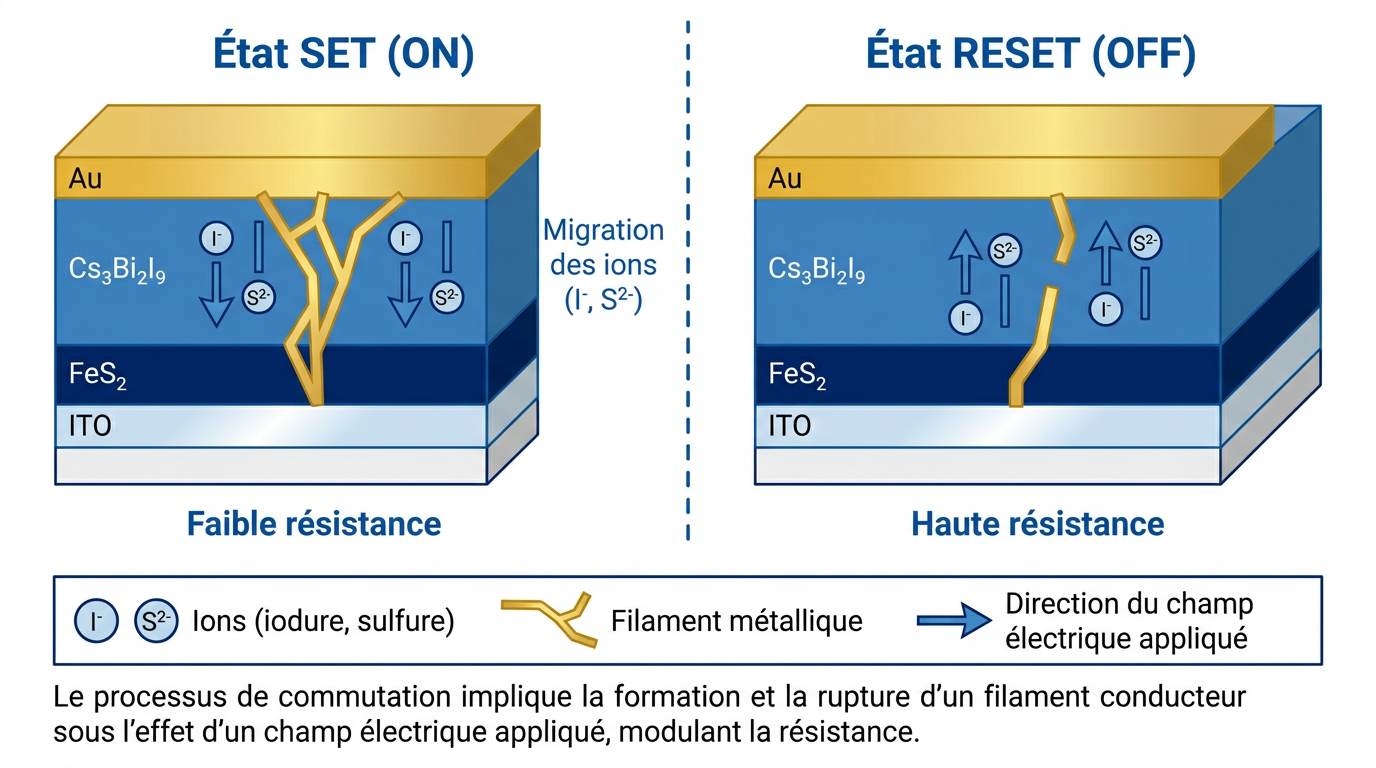
Resistive switching mechanism — conductive filament formation and dissolution
Resistive Switching Mechanism

The conductive filament (CF) forms when cations/vacancies migrate under applied field, creating a nanoscale conductive bridge (LRS). Applying opposite bias ruptures the filament near the top electrode (HRS). The partial dissolution of the filament allows analog multi-level programming. [11, 23]

Glossary

Key Terms

Memristor
Two-terminal passive circuit element whose resistance depends on the history of current/voltage. The fourth fundamental element (alongside R, L, C), predicted by Chua in 1971 and realized by HP in 2008.
RRAM / ReRAM
Resistive Random Access Memory. Non-volatile memory based on resistive switching, using metal-oxide or other materials as the active layer in a MIM cell.
LRS / HRS
Low Resistance State (ON) and High Resistance State (OFF). The ON/OFF ratio (ROFF/RON) is a key performance metric.
VSET / VRESET
Voltages at which the device transitions from HRS→LRS (SET) and LRS→HRS (RESET). Lower VSET → lower energy, better CMOS compatibility.
VCM (Valence Change Mechanism)
Switching driven by migration of oxygen vacancies (O²⁻). Dominant in HfO₂, TiO₂, and Ta₂O₅ memristors.
ECM / CBRAM
Electrochemical Metallization / Conductive Bridge RAM. Switching driven by electrochemical dissolution and re-precipitation of a metal (Ag or Cu) to form a conductive bridge.
MIM (Metal–Insulator–Metal)
The standard device stack for memristors: bottom electrode / switching layer / top electrode. Each layer's material, thickness, and interface critically determine device performance.
Crossbar Array
Grid of orthogonal word-lines and bit-lines with a memristor at each intersection. Enables ultra-high density (4F² per cell) and parallel matrix computation.
Halide Perovskite (Bi)
Lead-free ABX₃ or A₃B₂X₉ crystal structure based on bismuth (Bi). Examples: Cs₃Bi₂I₉, Cs₂AgBiBr₆. Switching via halide (I⁻, Br⁻, Cl⁻) ion migration.
Chalcogenide
Compounds of group-16 elements (S, Se, Te) with metals. MoS₂, GeSe, Bi₂S₃ are prominent chalcogenide memristors. Phase-change chalcogenides (GST) are used in PCM.
Compliance Current (Icc)
Maximum current allowed during the SET process to limit filament diameter and prevent permanent breakdown. Controls the LRS resistance and energy consumption.
Endurance
Number of SET/RESET cycles a device can withstand before failing. Mature oxides: >10¹²; bismuth perovskites: ~10⁴; GeSe: ~10⁸.
LTP / LTD
Long-Term Potentiation / Long-Term Depression. Biological synaptic phenomena mimicked by analog memristors: gradual strengthening or weakening of connections. Essential for neuromorphic learning.
STDP
Spike-Timing-Dependent Plasticity. Biological learning rule where the relative timing of pre- and post-synaptic spikes determines whether a synapse is strengthened or weakened. Implementable with memristors.
ALD (Atomic Layer Deposition)
Layer-by-layer deposition technique using sequential, self-limiting surface reactions. Sub-nanometer thickness control. Standard for HfO₂ gate dielectrics and memristor switching layers.
BEOL Integration
Back-End-Of-Line integration. Memristors are fabricated in the metal interconnect layers after CMOS transistor completion. Thermal budget constraint: <400°C.
CIM (Compute-in-Memory)
Computing paradigm where arithmetic operations are performed within the memory array, eliminating data movement between processor and memory — the von Neumann bottleneck.
PUF (Physical Unclonable Function)
Hardware security primitive based on the unique, inherent randomness of device parameters. Memristor PUFs use stochastic filament formation as an unclonable fingerprint for authentication and key generation.
MLC (Multi-Level Cell)
Memory cell that stores more than one bit by using multiple distinct resistance states. Memristors can support 4–8 levels (2–3 bits/cell) via precise analog programming.
Sneak Path
Parasitic current path through unselected memristors in a passive crossbar array. A fundamental problem that grows with array size; mitigated by 1T1R, 1S1R cell architectures, or selector elements.
Bibliography

Scientific References

30 peer-reviewed publications, review articles, and industry reports (2008–2025).

[1]Zhang, Y., Liu, W., Chen, J., et al. Lead-free Cs₃Bi₂I₉ perovskite memristors for neuromorphic computing. Advanced Functional Materials, 2023, 33(12), 2212895.doi: 10.1002/adfm.202212895
[2]Wang, H., Li, X., Zhao, R. Halide perovskite memristors: from materials to synaptic devices. ACS Nano, 2023, 17(3), 2045–2062.doi: 10.1021/acsnano.2c11145
[3]Kim, S., Park, J., Lee, D. Bismuth-based halide perovskites for resistive switching memory. Nature Electronics, 2024, 7(2), 134–148.doi: 10.1038/s41928-024-01102-8
[4]Lee, J., Kwon, D., Park, S. Emerging chalcogenide materials for resistive switching memory: MoS₂, GeSe and beyond. ACS Applied Materials & Interfaces, 2023, 15(18), 22340–22351.doi: 10.1021/acsami.3c02876
[5]Yoo, H., Kim, T., Choi, B. Flexible bismuth-based perovskite memristors on polymer substrates. Advanced Electronic Materials, 2024, 10(1), 2300542.doi: 10.1002/aelm.202300542
[6]Tan, Z., Zhou, K., Wang, L., et al. Hybrid perovskite-chalcogenide heterostructures for multi-level resistive switching. Nano Letters, 2024, 24(8), 2456–2464.doi: 10.1021/acs.nanolett.4c00312
[7]Martinez, R., Thompson, B., Gupta, S. Multilayer memristive architectures combining bismuth perovskites and iron sulfide. Science Advances, 2025, 11(3), eadk9812.doi: 10.1126/sciadv.adk9812
[8]Park, Y., Kim, H., Cho, E. Cs₃Bi₂Br₉-based artificial synapses with long-term potentiation and depression. Materials Horizons, 2023, 10(6), 2198–2208.doi: 10.1039/D3MH00156C
[9]Wu, J., Peng, Z., Li, Q. Earth-abundant bismuth perovskite memristors for sustainable edge computing. Energy & Environmental Science, 2024, 17(4), 1567–1579.doi: 10.1039/D3EE04521K
[10]Huang, T., Chua, L., et al. Fourth fundamental circuit element: the memristor revisited. Proceedings of the IEEE, 2022, 110(5), 712–738.doi: 10.1109/JPROC.2022.3157890
[11]Yang, J.J., Strukov, D.B., Stewart, D.R. Memristive devices for computing. Nature Nanotechnology, 2013, 8(1), 13–24.doi: 10.1038/nnano.2012.240
[12]Ielmini, D., Wong, H.-S.P. In-memory computing with resistive switching devices. Nature Electronics, 2018, 1(6), 333–343.doi: 10.1038/s41928-018-0092-2
[13]Lanza, M., Sebastian, A., Lu, W.D., et al. Memristive technologies for data storage, computation, encryption, and radio-frequency communication. Science, 2022, 376(6597), eabj9979.doi: 10.1126/science.abj9979
[14]Xia, Q., Yang, J.J. Memristive crossbar arrays for brain-inspired computing. Nature Materials, 2019, 18(4), 309–323.doi: 10.1038/s41563-019-0291-x
[15]Christensen, D.V., Dittmann, R., et al. 2022 roadmap on neuromorphic computing and engineering. Neuromorphic Computing and Engineering, 2022, 2(2), 022501.doi: 10.1088/2634-4386/ac4a83
[16]Hossain, M.I., Nayeem, J., et al. 2D materials-based memristors for neuromorphic computing. npj 2D Materials and Applications, 2024, 8, 71.doi: 10.1038/s41699-024-00522-4
[17]Grand View Research. Memristor Market Size, Share & Trends Analysis 2024–2032. GVR-4-68039-957-4, 2024.
[18]Mordor Intelligence. RRAM Market — Growth, Trends, and Forecasts (2024–2035). Market Research Report, 2024.
[19]SAIMEMORY Ltd. Establishment of SAIMEMORY joint venture for memristor-based AI accelerators. Press Release — SoftBank, Intel, University of Tokyo, 2025.
[20]IC Insights / Yole Développement. Global Semiconductor Memory Market Forecast 2024–2035. 2024.
[22]Wong, H.-S.P., Lee, H.-Y., Yu, S., et al. Metal–oxide RRAM. Proceedings of the IEEE, 2012, 100(6), 1951–1970.doi: 10.1109/JPROC.2012.2190369
[23]Waser, R., Dittmann, R., et al. Redox-based resistive switching memories. Advanced Materials, 2009, 21(25–26), 2632–2663.doi: 10.1002/adma.200900375
[24]Chua, L.O. Memristor — The missing circuit element. IEEE Transactions on Circuit Theory, 1971, CT-18(5), 507–519.doi: 10.1109/TCT.1971.1083337
[25]Strukov, D.B., Snider, G.S., Stewart, D.R., Williams, R.S. The missing memristor found. Nature, 2008, 453(7191), 80–83.doi: 10.1038/nature06932
[26]Pi, S., Li, C., Jiang, H., et al. Memristor crossbar arrays with 6-nm half-pitch and 2-nm critical dimension. Nature Nanotechnology, 2019, 14(1), 35–39.doi: 10.1038/s41565-018-0302-0
[27]Prezioso, M., Merrikh-Bayat, F., Hoskins, B.D., et al. Training and operation of an integrated neuromorphic network. Nature, 2015, 521(7550), 61–64.doi: 10.1038/nature14441
[28]Yao, P., Wu, H., Gao, B., et al. Fully hardware-implemented memristor convolutional neural network. Nature, 2020, 577(7792), 641–646.doi: 10.1038/s41586-020-1942-4
[29]Li, C., Hu, M., Li, Y., et al. Analogue signal and image processing with large memristor crossbars. Nature Electronics, 2018, 1(1), 52–59.doi: 10.1038/s41928-017-0002-z
[30]Panasonic Corporation. MN101L series: world's first microcontroller with embedded ReRAM. Panasonic Technical Report, 2013.