UV Gas Laser Technology

TrinityPhoton

UV Laser Engraving System

High-precision semiconductor processor engraving using UV gas laser technology with nanometric resolution and complete optical system integration.

System Overview

Advanced UV gas laser engraving for semiconductor processor fabrication with complete optical path control.

UV Gas Laser Source

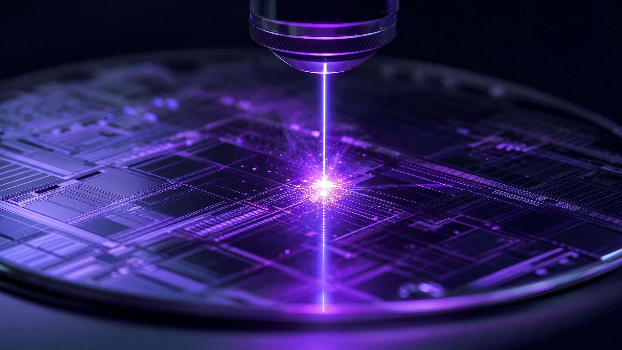
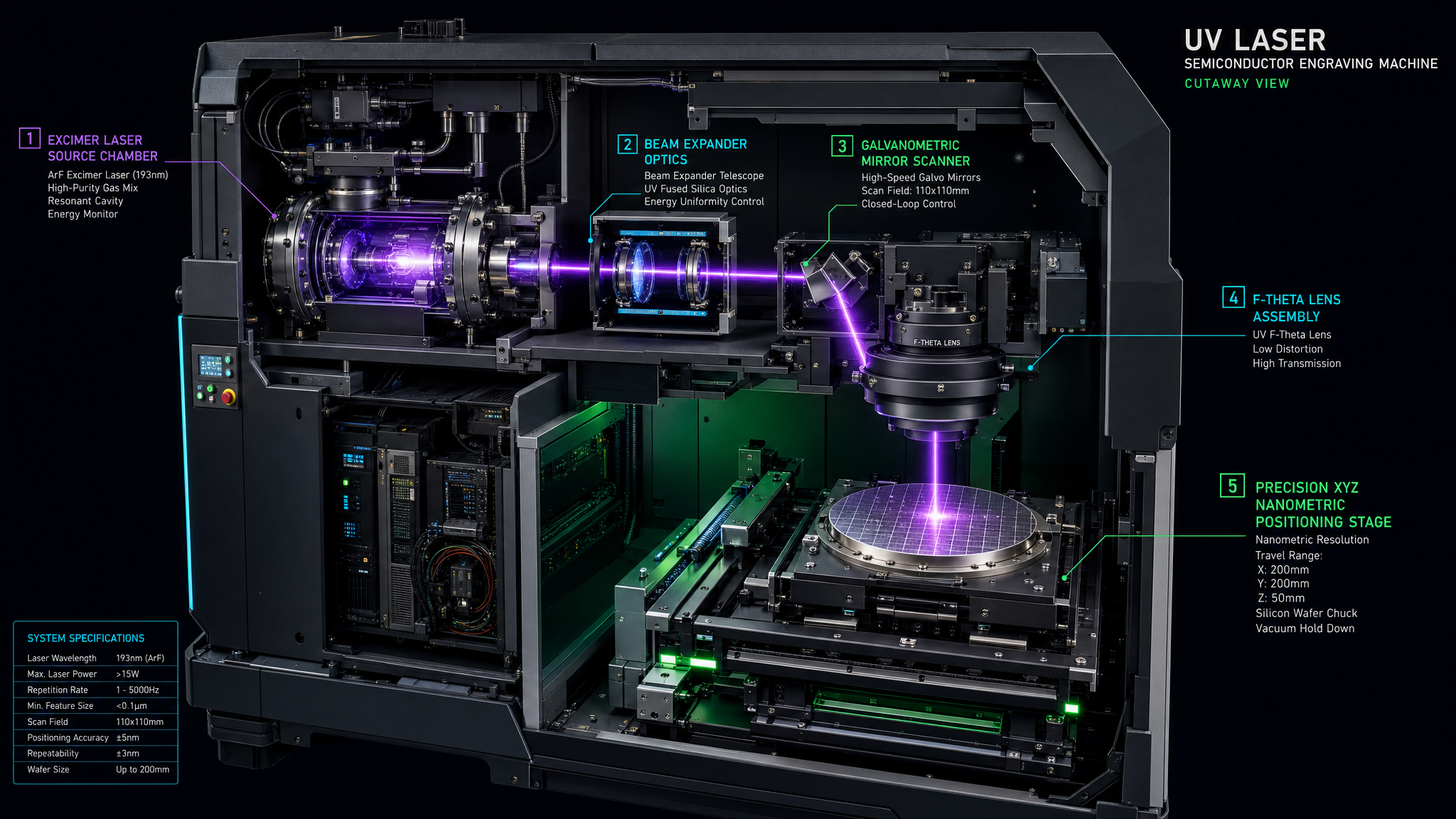
Excimer laser (KrF 248nm / ArF 193nm) delivering deep ultraviolet radiation for sub-micron ablation of semiconductor materials with minimal thermal impact.

Precision Optical System

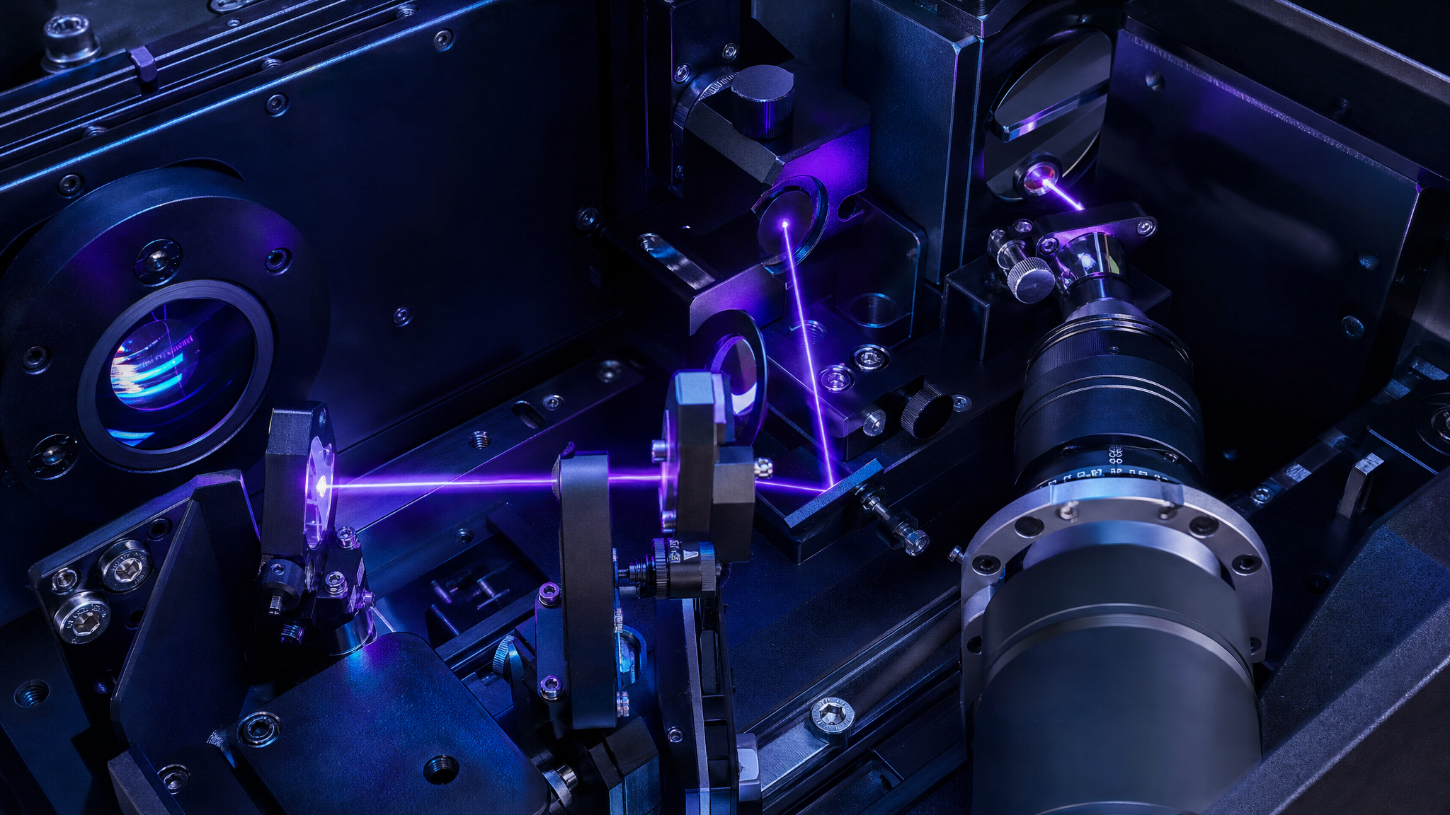
Galvanometric mirrors, f-theta scan lenses, and collimated beam path ensure diffraction-limited spot sizes below 500nm across the entire work field.

Nanometric Positioning

XYZ nanometric stage with ±10nm positioning accuracy, real-time FPGA control, and coaxial vision system for sub-wavelength alignment precision.

Cleanroom Compatible

Full N₂/Ar gas purge system, particle-free optical path, and ISO-class cleanroom integration for semiconductor fabrication environments.

The Machine

A deep look inside the TrinityPhoton system — engineered to the standards that power the world's most advanced semiconductor fabs.
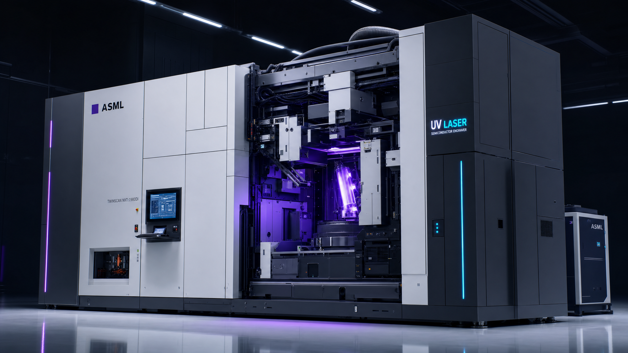
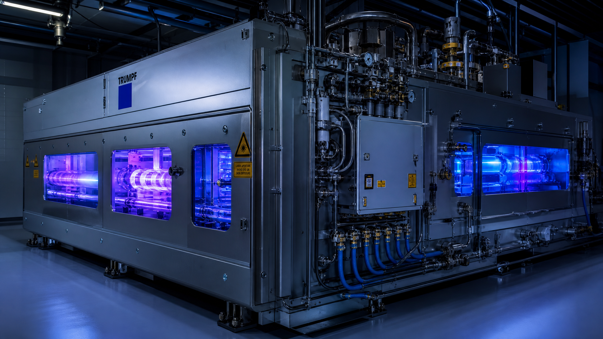
TrinityPhoton TP-193 full-scale UV laser semiconductor engraving machine in a cleanroom

TrinityPhoton TP-193 DUV Direct-Write Scanner

A full-scale deep-ultraviolet laser engraving platform for direct-write processor patterning. Weighing over 4,200 kg and standing 2.4 m tall, the TP-193 houses the complete beam chain — from the excimer gas source to the nanometric wafer stage — inside a vibration-isolated, cleanroom-grade enclosure.

193 nm
ArF DUV wavelength
< 500 nm
Focused spot size
± 10 nm
Stage repeatability
6,000 Hz
Pulse repetition rate

German-Engineered Optical Heritage

The TrinityPhoton architecture follows the same deep-tech lineage that defines the most advanced lithography tools running in Taiwan's leading foundries. The global standard — the EUV and DUV scanners integrated by ASML (Netherlands) — is built on two German pillars: TRUMPF, which builds the world's most powerful pulsed industrial lasers, and ZEISS SMT, whose reflective and refractive optics are the most precise ever manufactured. TrinityPhoton adopts this proven division of expertise — a high-power, gas-based DUV source paired with ultra-precision beam-shaping optics — and packages it into a compact direct-write engraving platform for processor fabrication and research.

TRUMPF-class laser sourceHigh-power pulsed gas laser architecture — the same discipline behind the EUV drive lasers used at TSMC.
ZEISS-grade opticsSub-nanometer surface figure mirrors and lenses; wavefront error held below λ/10.
ASML-style integrationFull system integration philosophy: source, optics and motion fused into one vacuum-clean beam path.
Deployed in Taiwan-class fabsEngineering standards aligned with the tools driving 5nm / 3nm / 2nm production nodes.

Physical Principles

The fundamental physics governing UV laser-matter interaction and optical system design.

Beer-Lambert Law

I(z) = I₀ · e^(−αz)

Describes UV laser absorption in semiconductor materials. α is the absorption coefficient, z is the penetration depth. At 248nm, silicon exhibits α > 10⁶ cm⁻¹.

Rayleigh Diffraction Limit

d = 1.22 · λ / NA

Minimum resolvable feature size. With λ = 248nm and NA = 0.6, theoretical resolution reaches ~500nm, enabling sub-micron processor engraving.

Laser Irradiance

I = P / A = P / (π·w²)

Power density at the focal point. Focused excimer beams achieve irradiance > 10⁸ W/cm², sufficient for ablative material removal.

Photon Energy

E = h·ν = h·c / λ

At 248nm, photon energy is 5.0 eV — exceeding the bond energy of Si-Si (3.4 eV), enabling direct photochemical bond breaking without thermal damage.

Optical Path Length

OPL = Σ nᵢ · dᵢ

Total optical path through the beam delivery system. Precise control ensures wavefront quality < λ/10 for diffraction-limited performance.

Process Science

The physics and chemistry of deep-UV laser ablation — how a 193 nm photon removes matter atom by atom while preserving the surrounding crystal.

01

Photon Absorption

The DUV pulse is absorbed within the first tens of nanometers of the substrate. At 193 nm the absorption coefficient of silicon exceeds 10⁶ cm⁻¹, so energy is deposited in an ultra-thin surface layer rather than heating the bulk.

02

Bond Dissociation

Each 193 nm photon carries 6.4 eV — more than the Si–Si (3.4 eV) or C–C bond energy. Bonds are broken directly (photochemically) rather than by heat, which is why the process is described as "cold" ablation.

03

Ablation Threshold

Material is removed only above a fluence threshold Fₜₕ. Below it, no net removal occurs; just above it, a precise, self-limiting layer is ejected per pulse — giving nanometer depth control.

04

Plume Ejection

The dissociated material leaves as a supersonic plasma plume, carrying away the deposited energy. This convective removal is what keeps the heat-affected zone (HAZ) below ~100 nm.

05

Layer-by-Layer Etch

Repeating the pulse at 1–6,000 Hz removes calibrated depth per shot. Combined with galvo scanning, arbitrary 2.5D patterns are written with sub-500 nm lateral resolution.

06

In-situ Metrology

Coaxial vision and an in-line power sensor close the loop: pulse energy, spot position and etched depth are monitored in real time and corrected by the FPGA controller.

Governing Process Model

The etch depth per pulse follows the classic logarithmic ablation law derived from Beer–Lambert absorption:

d = (1/α) · ln(F / Fₜₕ)

where d is depth removed per pulse, α the effective absorption coefficient, F the applied fluence and Fₜₕ the ablation threshold. This equation, combined with the Rayleigh diffraction limit for lateral resolution, fully describes the achievable 2.5D geometry.

Key Process Parameters

Fluence (F)0.1 – 5 J/cm²

Energy density per pulse; sets etch depth per shot above threshold.

Ablation threshold (Fₜₕ)~ 0.3 J/cm² (Si)

Minimum fluence for net material removal.

Etch rate20 – 300 nm/pulse

Increases logarithmically with fluence (Beer–Lambert regime).

Heat-affected zone< 100 nm

Minimised by short DUV absorption depth and plume convection.

Pulse duration10 – 30 ns

Excimer regime — short enough to avoid thermal diffusion into the bulk.

Beam overlap50 – 90 %

Pulse-to-pulse overlap controlling surface roughness and uniformity.

Technical Components

Every precision component engineered for optimal UV laser beam delivery and semiconductor processing.

UV Gas Laser Source

Excimer KrF 248nm / ArF 193nm, pulsed UV emission, > 10⁹ shot lifetime

Galvanometric Mirror

High-speed dual-axis scanning mirrors, < 0.5ms settling time, ±20° range

F-Theta Scan Lens

Telecentric f-theta lens for flat-field focusing across 300×300mm work area

Beam Collimation System

Multi-element collimator ensuring < 0.5 mrad divergence over full beam path

Variable Attenuator

Motorized energy control with 0.1% resolution for precise fluence adjustment

Beam Expander

Galilean telescope design, 2x–10x expansion ratio, AR-coated for DUV

Projection Mask (Reticle)

Chrome-on-quartz photomask for complex pattern projection lithography

XYZ Nanometric Stage

Piezo-driven stage, ±10nm precision, 300×300mm travel, air-bearing design

Gas Purge System

N₂/Ar purge maintaining < 1 ppm O₂ in beam path for DUV transmission

FPGA Real-Time Controller

Sub-microsecond synchronization of laser, scanner, and stage positioning

Coaxial Vision Camera

Through-the-lens alignment camera with sub-pixel pattern recognition

In-Line Power Sensor

Real-time pulse energy monitoring with ±0.5% accuracy at full rep rate

Technical Specifications

Detailed performance parameters of the TrinityPhoton UV laser engraving system.

TrinityPhoton UV System
Wavelength193 nm / 248 nm / 351 nm
Peak PowerUp to 50 W
Spot Size< 500 nm
Pulse Rate1 – 6,000 Hz
Positioning Accuracy± 10 nm
Work Area300 × 300 mm
Engraving Depth10 nm – 50 μm
Compatible MaterialsSi, GaAs, SiC, LiNbO₃, Glass, Polymers
Laser Lifetime> 1 × 10⁹ pulses

Performance Analytics

Quantitative performance data demonstrating TrinityPhoton's superior capabilities.

Resolution vs Wavelength

0.3 ArF 193nm 0.5 KrF 248nm 1.0 UV 355nm 2.5 Visible 532nm 5.0 IR 1064nm 25 CO₂ 10.6μm Resolution (μm, log scale)

Engraving Depth vs Fluence

0 25k 50k 0.5 5 10 15 20 Fluence (J/cm²)

Engraving Speed by Material

Si
95%
GaAs
85%
SiC
60%
LiNbO₃
70%
Glass
80%
Polymer
100%

Technology Comparison

How TrinityPhoton UV laser technology compares to alternative engraving methods.

Criteria TrinityPhoton UV CO₂ Laser Fiber Laser E-Beam
Resolution
Speed
Cost
Material Compatibility
Precision
Work Area
Maintenance

Advantages & Limitations

Advantages

  • Nanometric resolution (< 500 nm)
  • Non-contact processing
  • Semiconductor-compatible materials
  • Minimal Heat Affected Zone (HAZ)
  • Programmable CNC patterns
  • Multi-material versatility
  • Cleanroom-grade operation

Limitations

  • High initial investment
  • Excimer gas maintenance
  • Controlled environment required
  • Specialized training needed

Applications

Industries and research domains leveraging TrinityPhoton UV laser engraving.

Semiconductor Fabrication

Direct-write lithography for processor and IC patterning at sub-micron scales.

Microelectronics R&D

Rapid prototyping of circuit designs and experimental device structures.

Photonics & Optoelectronics

Waveguide fabrication, grating inscription, and photonic crystal patterning.

MEMS / NEMS

Micro/nano-electromechanical system fabrication with high aspect ratios.

University Laboratories

Research-grade tool for academic institutions studying laser-matter interactions.

Aerospace Industry

Precision marking and micro-machining of aerospace-grade materials and sensors.

Implantable Medical Devices

Biocompatible surface texturing and micro-patterning for medical implants.

Engineering & Design Process

From optical simulation to system delivery — our rigorous engineering pipeline.

01

Optical Simulation

Zemax/Code V ray-tracing and beam propagation modeling for optimal optical train design.

02

Mechanical Design

Precision opto-mechanical CAD engineering with thermal and vibration analysis.

03

System Integration

Assembly of laser source, beam delivery, scanning optics, and motion stages.

04

Calibration

Wavefront measurement, beam profiling, and power calibration across all operating modes.

05

Validation

Engraving test matrices on reference substrates with SEM/AFM metrology verification.

06

Delivery

Installation, cleanroom integration, operator training, and ongoing technical support.

Evidence Quality & Validation Gates

This platform mixes mature UV-laser engineering with forward-looking performance assumptions. The matrix below distinguishes what is established from what still requires campaign-level verification.

High-confidence foundation

Excimer-laser physics, beam-delivery optics, cleanroom process controls, and in-line metrology are mature industrial domains with well-documented implementation patterns.

Model-dependent claims

Throughput, yield, and cost-performance metrics depend strongly on substrate class, resist stack, uptime assumptions, and integration quality across the full toolchain.

Critical KPIs

CD uniformity, edge roughness, overlay error, defect density, and uptime should be tracked with p50/p95 bands across representative production and R&D workloads.

Operational constraints

Gas handling, optical contamination, thermal drift, and maintenance cadence can dominate lifecycle economics unless monitored by strict preventive quality protocols.

References & Further Reading

Peer-reviewed literature and industry sources underpinning the science and technology of DUV laser processing and semiconductor lithography.

Laser–Matter Interaction & Ablation

Bäuerle, D. — Laser Processing and Chemistry, 4th ed., Springer (2011).

Reference textbook on photochemical and photothermal laser ablation mechanisms.

Ihlemann, J., Wolff, B., Simon, P. — "Nanosecond and femtosecond excimer laser ablation of fused silica", Applied Physics A 54 (1992) 363–368.

Foundational study on DUV excimer ablation thresholds.

Srinivasan, R., Braren, B. — "Ultraviolet laser ablation of organic polymers", Chemical Reviews 89 (1989) 1303–1316.

Origin of the logarithmic ablation-depth law.

Semiconductor Lithography & Optics

Bakshi, V. (ed.) — EUV Lithography, 2nd ed., SPIE Press (2018).

Comprehensive reference on advanced UV/EUV lithography systems.

ZEISS SMT — "EUV Lithography: Optics for the most advanced chips", ZEISS Semiconductor Manufacturing Technology (2023).

Sub-nanometer mirror figuring and projection optics.

TRUMPF — "EUV drive laser: the world's most powerful pulsed industrial laser", TRUMPF Technical Documentation (2023).

High-power pulsed gas-laser architecture.

Industry & Standards

ASML — "TWINSCAN NXE & NXT platforms", ASML Product Documentation (2023).

System-integration reference for DUV/EUV scanners deployed in Taiwan-class fabs.

SEMI Standards — "Guide for cleanroom classification and laser safety in semiconductor fabs", SEMI International Standards.

Cleanroom and DUV laser-safety practice.

Fraunhofer ILT — "Micromachining with UV and ultrashort-pulse lasers", Fraunhofer Institute for Laser Technology (2022).

Applied process research on precision UV micromachining.

TrinityPhoton is a conceptual precision-engineering platform. References are provided to document the established physics and industry practices on which the technology is based; company and product names are the property of their respective owners.

← Back to Humanity · A Maxware project